- 您现在的位置:买卖IC网 > Sheet目录1991 > CS4461-CZZR (Cirrus Logic Inc)IC ADC PSR FEEDBACK 24-TSSOP
4
DS650F1
CS4461
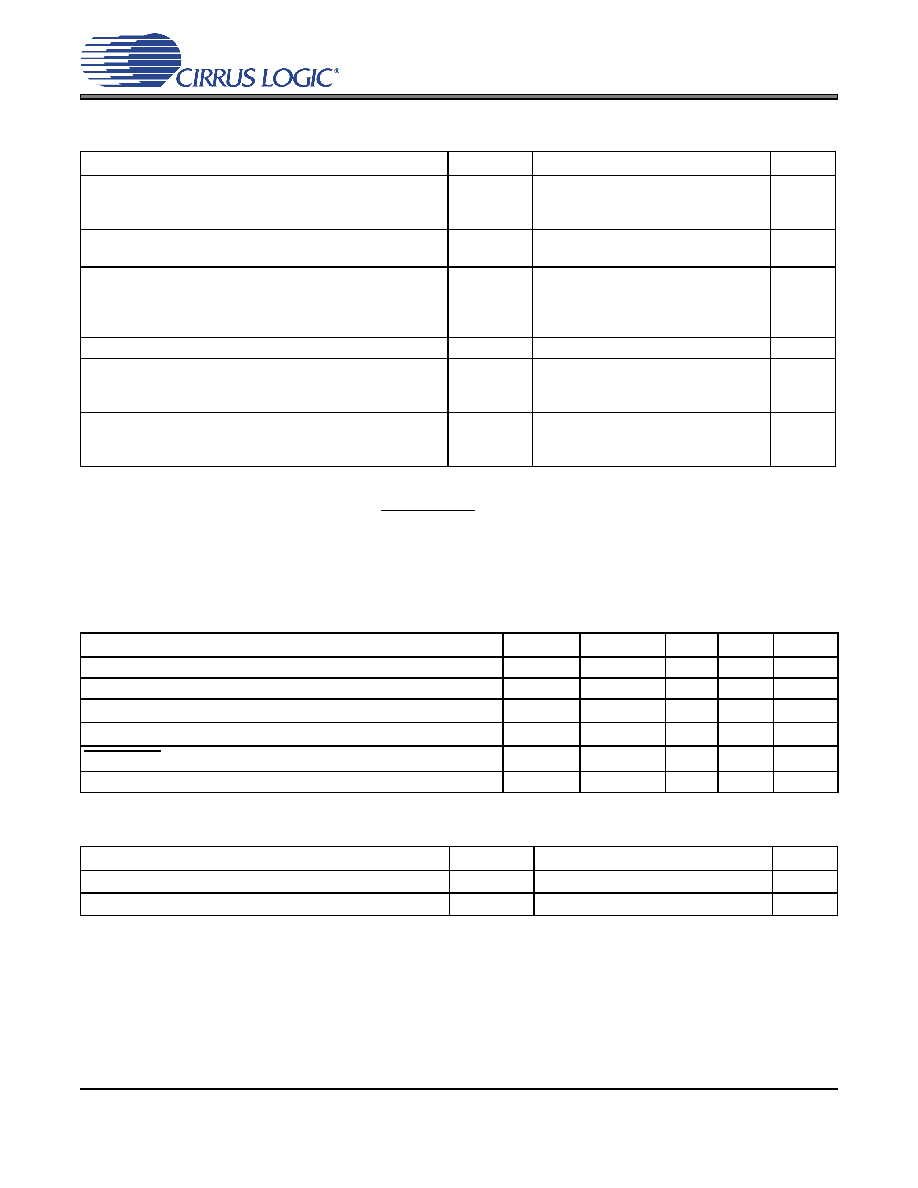
DC ELECTRICAL CHARACTERISTICS
(GND = 0 V, all voltages with respect to ground.
PSR_MCLK=12.288 MHz)
Notes:
4. Power Down Mode is defined as PSR_RESET = Low with all clocks and data lines held static.
5. Valid with the recommended capacitor values on FILT+ and VQ as shown in the Typical Connection
DIGITAL CHARACTERISTICS
THERMAL CHARACTERISTICS
Parameter
Symbol
Min
Typ
Max
Unit
Power Supply Current
VA
(Normal Operation)
VDP = 5.0 V
VDP = 3.3 V
IA
ID
-
17.5
22
14.5
21
26
17
mA
Power Supply Current
VA
(Power-Down Mode) (Note 4)
VDP = 5.0 V
IA
ID
-
2
-
mA
Power Consumption
(Normal Operation)
VDP = 5.0 V
VDP = 3.3 V
(Power-Down Mode)
VDP = 5.0 V
-
198
135
20
235
161
-
mW
ADC Power Supply Rejection Ratio (1 kHz)
PSRR
-
65
-
dB
VQ Nominal Voltage
Output Impedance
Maximum allowable DC current source/sink
-
2.5
25
0.01
-
V
k
mA
FILT+ Nominal Voltage
Output Impedance
Maximum allowable DC current source/sink
-
5
18
0.01
-
V
k
mA
Parameter
Symbol
Min
Typ
Max
Units
High-Level Input Voltage
(% of VDP)
VIH
70%
-
V
Low-Level Input Voltage
(% of VDP)
VIL
--
30%
V
High-Level Output Voltage at Io = 100 A
(% of VDP)
VOH
70%
-
V
Low-Level Output Voltage at Io = 100 A
(% of VDP)
VOL
--
15%
V
OVERFLOW Current Sink
IOVERFLOW
--
4.0
mA
Input Leakage Current
Iin
--
±10
A
Parameter
Symbol
Min
Typ
Max
Unit
Allowable Junction Temperature
-
135
°C
Junction to Ambient Thermal Impedance
θJA
-70
-
°C/W
发布紧急采购,3分钟左右您将得到回复。
相关PDF资料
CS5340-CZZ
IC ADC AUD 101DB 200KHZ 16-TSSOP
CS5340-DZZR
IC ADC AUD 101DB 200KHZ 16-TSSOP
CS5341-DZZ
IC ADC AUD 105DB 200KHZ 16-TSSOP
CS5342-CZZ
IC ADC AUD 105DB 200KHZ 16-TSSOP
CS5345-CQZ
IC ADC AUD 104DB 200KHZ 48-LQFP
CS5345-DQZ
IC ADC AUD 104DB 200KHZ 48-LQFP
CS5346-CQZR
IC ADC AUD 103DB 200KHZ 48-LQFP
CS5351-BZZ
IC ADC AUD 108DB 204KHZ 24-TSSOP
相关代理商/技术参数
CS4461-DZZ
制造商:Cirrus Logic 功能描述:ADC SGL DELTA-SIGMA 7.5MSPS SERL 24TSSOP - Rail/Tube
CS4461-DZZR
制造商:Cirrus Logic 功能描述:ADC SGL DELTA-SIGMA 7.5MSPS SERL 24SSOP - Tape and Reel
CS4468A3
制造商:HVPSI 制造商全称:High Voltage Power Solutions, Inc. 功能描述:180 KV RECTIFIER
CS4473-000
制造商:TE Connectivity 功能描述:MTC100-JA2-P11M2-CS082 - Bulk
CS4474-000
制造商:TE Connectivity 功能描述:Connector Accessories Socket Insert 制造商:TE Connectivity 功能描述:MTC100-JA2-S11M2-CS082 - Bulk
CS4475-000
制造商:TE Connectivity 功能描述:Connector Accessories Pin Insert 制造商:TE Connectivity 功能描述:MTC100-EA2-P12M1-CS082 - Bulk
CS4476-000
制造商:TE Connectivity 功能描述:MTC100-EA2-S12M1-CS082 - Bulk
CS4477-000
制造商:TE Connectivity 功能描述:Connector Accessories Pin Insert 制造商:TE Connectivity 功能描述:MTC100-EA2-P12M2-CS082 - Bulk